Activity 2.1.1 AOI Design: Truth Tables to Logic Expressions
The first step in designing a new product is clearly defining the design requirements or design specifications. These design specifications detail all of the features and limitations of the new product.
In digital electronics, the process of translating these design specifications into a functioning circuit starts with the creation of a truth table. A truth table is simply a list of all possible binary input combinations that could be applied to a circuit and the corresponding binary outputs that the circuit produces. Once the truth table is complete, a Boolean expression can easily be written directly from the truth table.
In this activity you will learn how to translate design specifications into truth tables and, in turn, write un-simplified logic expressions from these truth tables.
In future activities we will learn how to use Boolean algebra as well as a graphical technique called Karnaugh mapping to simplify these logic expressions.
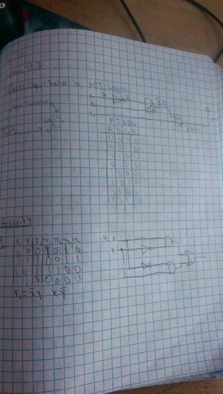
Activity 2.1.2 AOI Logic Analysis: Circuit to Truth Table to Logic Expression
What does this circuit do? Does the circuit that I designed work? If you are able to analyze AOI logic circuits, you will be able to answer these questions. The first question frequently comes up when you need to determine the functionality of a previously designed circuit. The second question will always need to be answered whenever you design a new logic circuit.
When you analyze an AOI logic circuit, you can use one of two techniques. With the first technique, you determine the circuit’s truth table from which the output logic expression is derived. With the second technique, the order is reversed. The circuit’s logic expression is determined. The truth table is then derived using this expression.
In this activity you will learn how to analyze AOI logic circuits to determine the circuit truth table and output logic expression
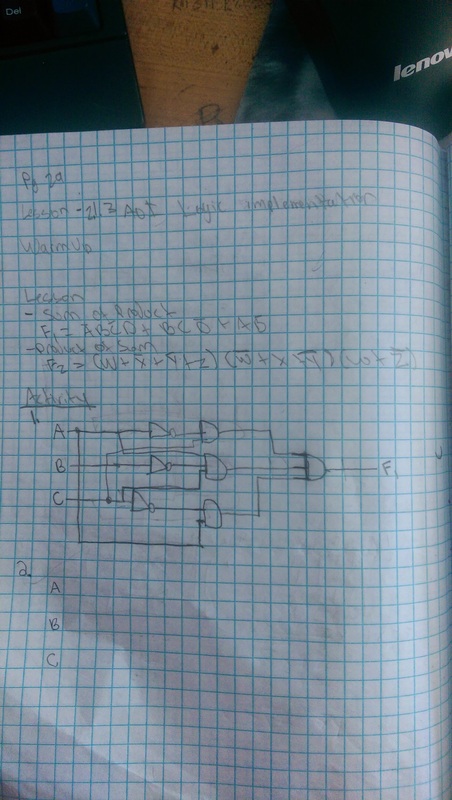
Activity 2.1.3 AOI Logic Implementation
Would you pay $199 for a written specification for an MP3 player? Would you pay $299 for the schematics for a cell phone? Of course not. You don’t pay for the specifications or the schematics; you pay for the product itself.
You are not quite to the point where you can design an MP3 player or a cell phone, but you can design AOI logic circuits. In this activity you will learn how to implement AOI logic circuits from logic expressions. The logic expressions will be in either Sum-Of-Products (SOP) or Product-Of-Sums (POS) form.
You are not quite to the point where you can design an MP3 player or a cell phone, but you can design AOI logic circuits. In this activity you will learn how to implement AOI logic circuits from logic expressions. The logic expressions will be in either Sum-Of-Products (SOP) or Product-Of-Sums (POS) form.
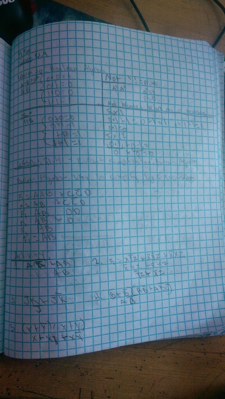
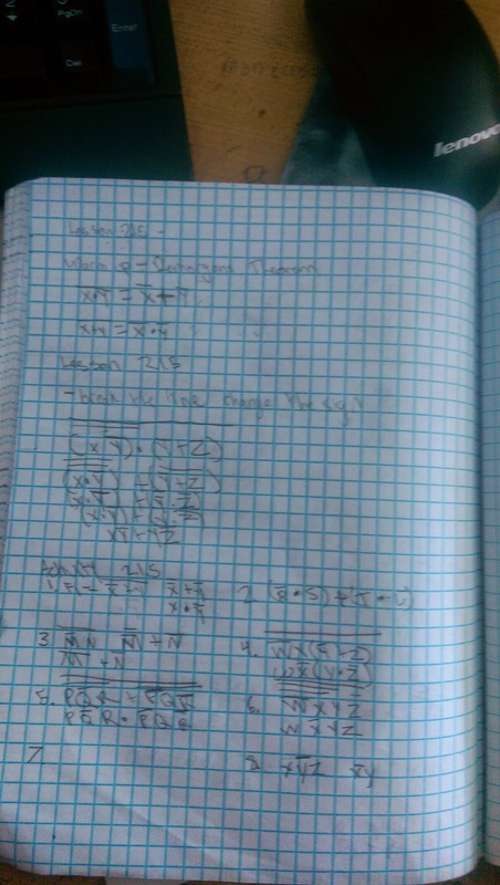
Activity 2.1.4 Circuit Simplification: Boolean Algebra
Have you ever had an idea that you thought was so unique that when you told someone else about it, you simply could not believe they thought you were wasting your time with it? If so, you know how the mathematician George Boole felt in the 1800s when he designed a math system that, at the time, had no practical application. Today, however, his math system is the most important mathematical tool used in the design of digital logic circuits. Boole introduced the world to Boolean algebra when he published his work called “An Investigation of the Laws of Thought, on Which Are Founded the Mathematical Theories of Logic and Probabilities.”
In the same way that normal algebra has rules that allow you to simplify algebraic expressions, Boolean algebra has theorems and laws that allow you to simplify expressions used to create logic circuits.
By simplifying the logic expression, we can convert a logic circuit into a simpler version that performs the same function. The advantage of a simpler circuit is that it will contain fewer gates, will be easier to build, and will cost less to manufacture.
In this activity you will learn how to apply the theorems and laws of Boolean algebra to simplify logic expressions and digital logic circuits.
The moral of the story is to keep dreaming. Someday your grandchildren may be using something that you’re thinking about right now. When your grandparents were kids, do you think that they imagined someday that we would all have 10,000 songs in our pockets or a telephone in our backpacks?
Activity 2.1.5 Circuit Simplification: DeMorgan's Theorems
Despite all of the work done by George Boole, there was still more work to be done. Expanding on Boole’s studies, Augustus DeMorgan (1806-1871) developed two additional theorems that now bear his name. Without DeMorgan’s Theorems, the complete simplification of logic expression would not be possible.
As we will seen in later activities, DeMorgan’s Theorems are the foundation for the NAND and NOR logic gates. In this activity you will learn how to simplify logic expressions and digital logic circuits using DeMorgan’s two theorems along with the other laws of Boolean algebra.
As we will seen in later activities, DeMorgan’s Theorems are the foundation for the NAND and NOR logic gates. In this activity you will learn how to simplify logic expressions and digital logic circuits using DeMorgan’s two theorems along with the other laws of Boolean algebra.
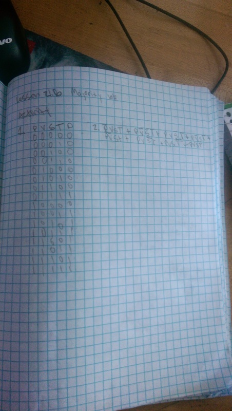
Project 2.1.6 AOI LogicDesign: Majority Vote
The United States 2000 Presidential Election between George W. Bush (Republican) and Albert "Al" Gore (Democrat) will be best remembered for the controversy over who won Florida's 25 electoral votes, and ultimately, who won the presidency.
At the heart of the controversy was the use of antiquated and unreliable paper ballots. The use of these paper ballots resulted in an unacceptable amount of over-votes and under-votes. An over-vote occurs when someone’s vote is counted more than once, and an under-vote occurs when someone’s vote is not counted at all.
To ensure that this type of controversy does not occur at your company, the board of directors has asked you to design an electronic voting machine. The voting machine will allow the four board members to cast their ballots and will display the pass/fail status of each of their decisions.
The board of directors has four members; a president, a vice-president, a secretary, and a treasurer. Each member has a single yes/no vote. For a decision to pass, a majority of the board members must vote yes. In the event of a tie, the president’s vote is used to break the tie (i.e., if the president votes yes, the decision passes. If the president votes no, the decision fails.).
In this project, you will use only AND, OR & Inverter logic gates, frequently referred to as AOI logic, to design, simulate, and build a Majority Vote voting machine that meets these design specifications.
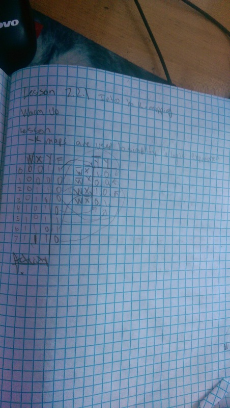
Activity 2.2.1 Circuit Simplification: Karnaugh Mapping
At this point you have the ability to apply the theorems and laws of Boolean algebra to simplify logic expressions in order to produce simpler and more cost effective digital logic circuits. You may have also realized that simplifying a logic expression using Boolean algebra, though not terribly complicated, is not always the most straightforward process. There isn’t always a clear starting point for applying the various theorems and laws, nor is there a definitive end in the process.
Wouldn’t it be nice to have a process for simplifying logic expressions that was more straightforward, had a clearly defined beginning, middle, and end, and didn’t require you to memorize all of the Boolean theorems and laws? Well there is, and it’s called Karnaugh mapping. Karnaugh mapping, or K-Mapping, is a graphical technique for simplifying logic expressions containing up to four variables.
In this activity you will learn how to utilize the Karnaugh mapping technique to simplify two, three, and four variable logic expressions. Additionally, logic expressions containing don’t care conditions will be simplified using the K-Mapping process.
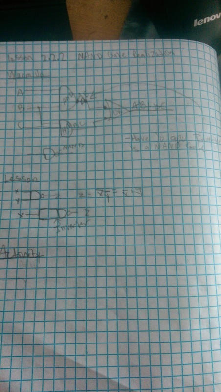
Activity 2.2.2 Universal Gates: NAND Only
The block diagram shown below represents a voting booth monitoring system. For privacy reasons, a voting booth can only be used if the booth on either side is unoccupied. The monitoring system has four inputs and two outputs. Whenever a voting booth is occupied, the corresponding input (A, B, C, & D) is a (1). The first output, Booth, is a (1) whenever a voting booth is available. The second output, Alarm, is a (1) whenever the privacy rule is violated.
In this activity you will implement NAND only combinational logic circuits for the two outputs Booth and Alarm. These NAND only designs will be compared with the original AOI implementations in terms of efficiency and gate/IC utilization. In a future activity, these NAND only designs will be compared to the circuits implemented using only NOR gates.
In this activity you will implement NAND only combinational logic circuits for the two outputs Booth and Alarm. These NAND only designs will be compared with the original AOI implementations in terms of efficiency and gate/IC utilization. In a future activity, these NAND only designs will be compared to the circuits implemented using only NOR gates.
Activity 2.3.1 Hexadecimal and Octal Number Systems
We all know that digital electronics use the binary number system. However, with new computers containing 32, 64, and even 128 bit data busses, displaying numbers in binary is quite cumbersome. For example, a single piece of data on a 64-bit data bus would look like this:
0110100101110001001101001100101001101001011100010011010011001010
Obviously, presenting data in this form would invite error. For this reason we use the hexadecimal (base 16) and, to a lesser extent, the octal (base 8) number systems. In this activity you will learn how to convert numbers between the decimal, binary, octal, and hexadecimal number systems.
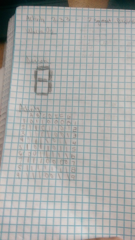
Activity 2.3.2 Seven Segment Displays
What do alarm clocks, cable TV converter boxes, home answering machines, and inexpensive calculators all have in common? In addition to being built from electronics, many also include seven-segment displays as part of their design.
There are two types of seven-segment displays: common cathode and common anode. Understanding how these displays work and the differences between them is fundamental to designing many different types of electronic devices. In this activity you will learn how to use seven-segment displays to display both alpha and numeric characters. You will also be introduced to the Seven-Segment Display Driver.
There are two types of seven-segment displays: common cathode and common anode. Understanding how these displays work and the differences between them is fundamental to designing many different types of electronic devices. In this activity you will learn how to use seven-segment displays to display both alpha and numeric characters. You will also be introduced to the Seven-Segment Display Driver.
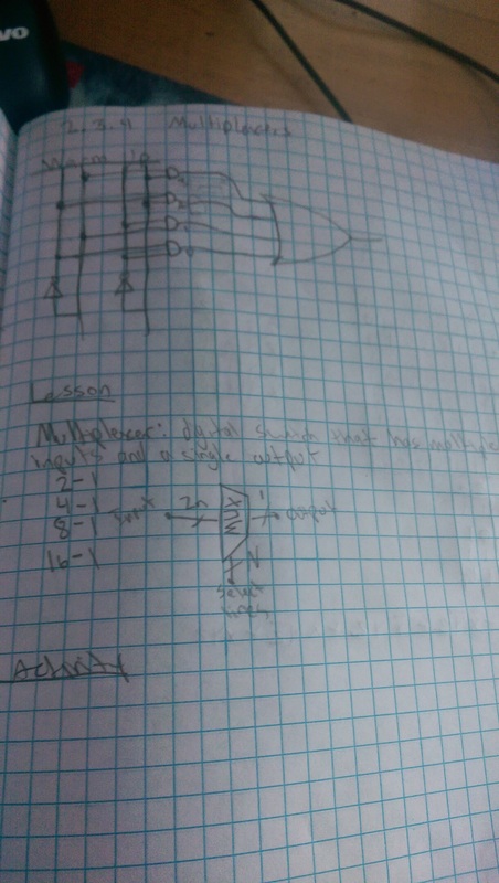
Activity 2.3.3 Multiplexers (MUX) and Demultiplexers (DEMUX)
Though it may be hard for you to believe, there was once a day when not everyone had a cell phone. Every house had one phone. That’s right, just one. How was this phone connected to all of the other phones in your town or country? Obviously it isn’t practical to have a wire from your phone connected directly to all other phones individually. This would require an unimaginable amount of wire traveling to and from every home in America. The solution to this problem is for a group of homes to share one wire with another group of homes. This is sharing of a resource and, in this case, the wire is a classic application of a multiplexer/de-multiplexer circuit.
Another classic application of multiplexing/demultiplexing is the way that seven-segment display signs are wired. In this activity you will implement two simple display signs. The first will not take advantage of multiplexing and the second will.
Another classic application of multiplexing/demultiplexing is the way that seven-segment display signs are wired. In this activity you will implement two simple display signs. The first will not take advantage of multiplexing and the second will.
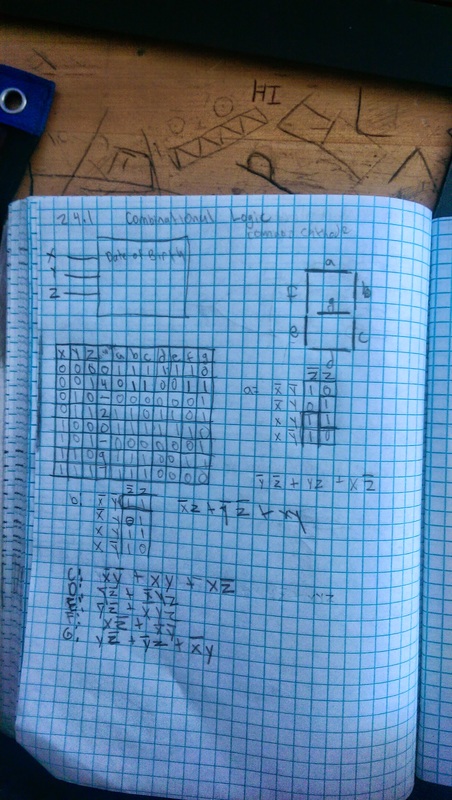
Problem 2.4.1 Combinational Logic Circuit Design: Date of Birth
The world’s first all-transistor calculator was the IBM 608. The 608 was introduced in 1955 at a cost of $83,210. The calculator was the size of a large dresser. The 608 was capable of addition, subtraction, multiplication, and division, the same capabilities of a four-function calculator that you can buy today at a store for $2.99. Despite the tremendous decrease in size and price that has occurred over the last five decades, the underlying design principles for the two calculators are the same.
In this activity you will implement an adder that combines two 2-bit numbers. This 2-bit adder design is a simplified version of the adder that is in a four-function calculator. You will implement both a small-scale integration (SSI) and medium-scale integration version of the 2-bit adder.
In this activity you will implement an adder that combines two 2-bit numbers. This 2-bit adder design is a simplified version of the adder that is in a four-function calculator. You will implement both a small-scale integration (SSI) and medium-scale integration version of the 2-bit adder.